

ShinePCB Manufacturing
Orders are coordinated through a partner-factory network in Dalian, Zhuhai, Shenzhen, Ningbo and Wuhan, with the assigned facility selected for the required process and qualification.
Precise allocation across a qualified network
Our Shenzhen branch coordinates each project. Based on product type, process, materials, quality system and capacity, the order is allocated to the facility in the ShinePCB manufacturing network whose capability and certification scope fit the requirements.
Partner factories are located in Dalian, Zhuhai, Shenzhen, Ningbo and Wuhan. The actual manufacturing entity, production scope, applicable certificates and supply-chain documentation are confirmed in the formal quotation and project documents.
Rigid PCB manufacturing flow
The standard rigid-board process from the ShinePCB company presentation.
Cutting
Laminate panels cut to working size.
Inner-layer imaging
Inner-layer patterns imaged and etched, then checked by AOI.
Lamination
Cores and prepregs pressed into the multilayer stack.
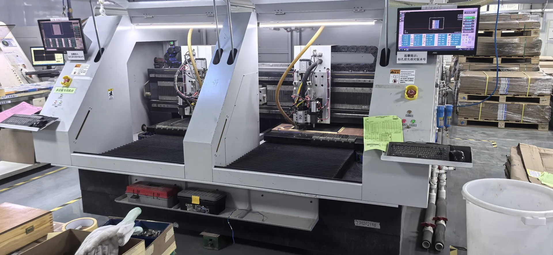
Drilling
Mechanical and laser drilling of holes and vias.
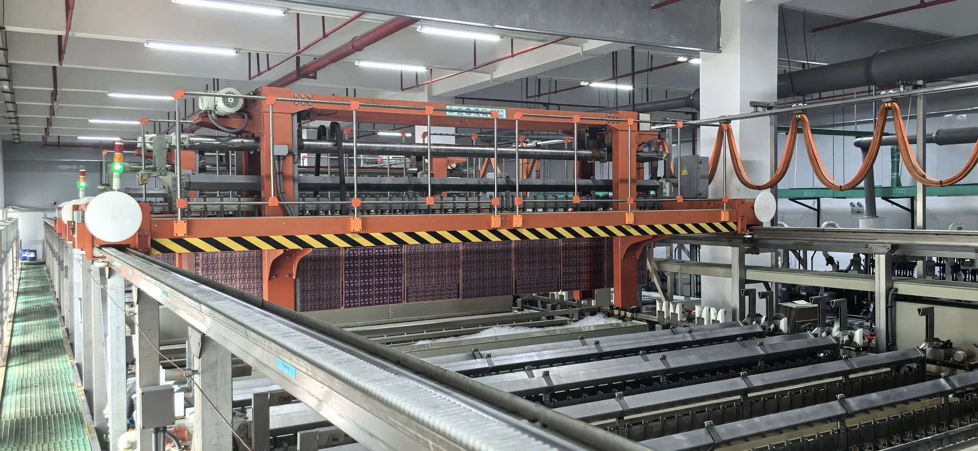
Plating
Hole metallization and copper plating.
Outer-layer imaging
Outer-layer patterns imaged, etched and checked by AOI.
Solder mask & legend
Solder mask and silkscreen applied.
Surface finish
ENIG, hard gold, immersion tin or silver, OSP and others.
Profiling
Routing, V-cut and outline machining.
Electrical test & final inspection
Flying-probe or fixture test, final inspection and packing.
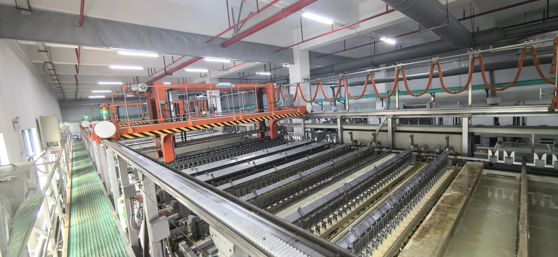
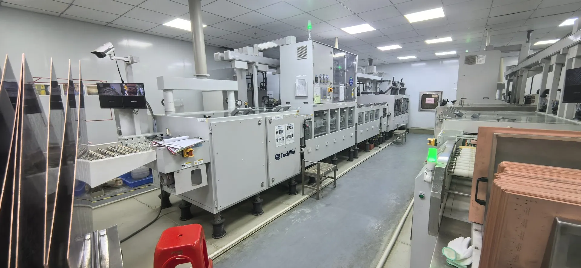
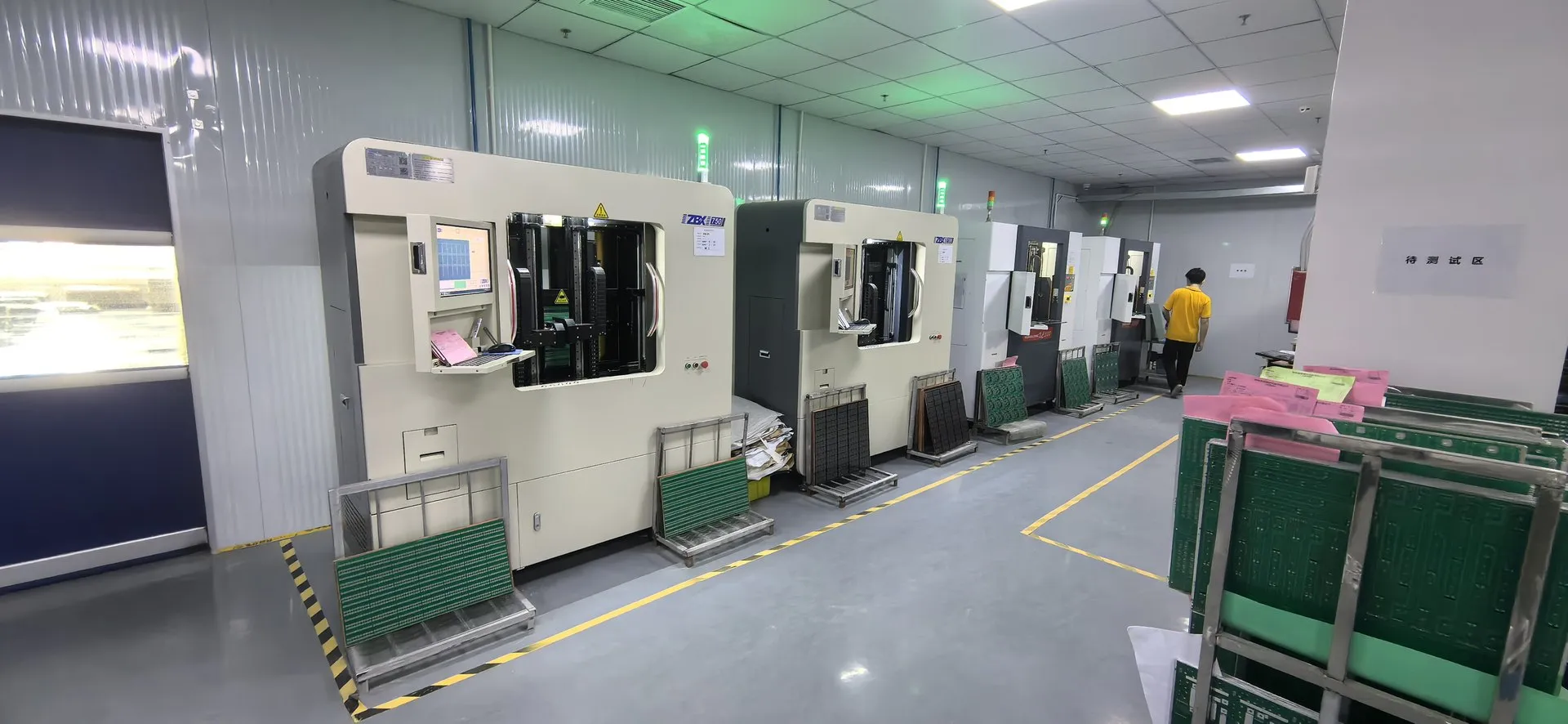
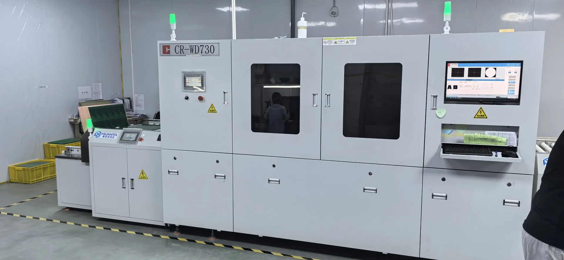
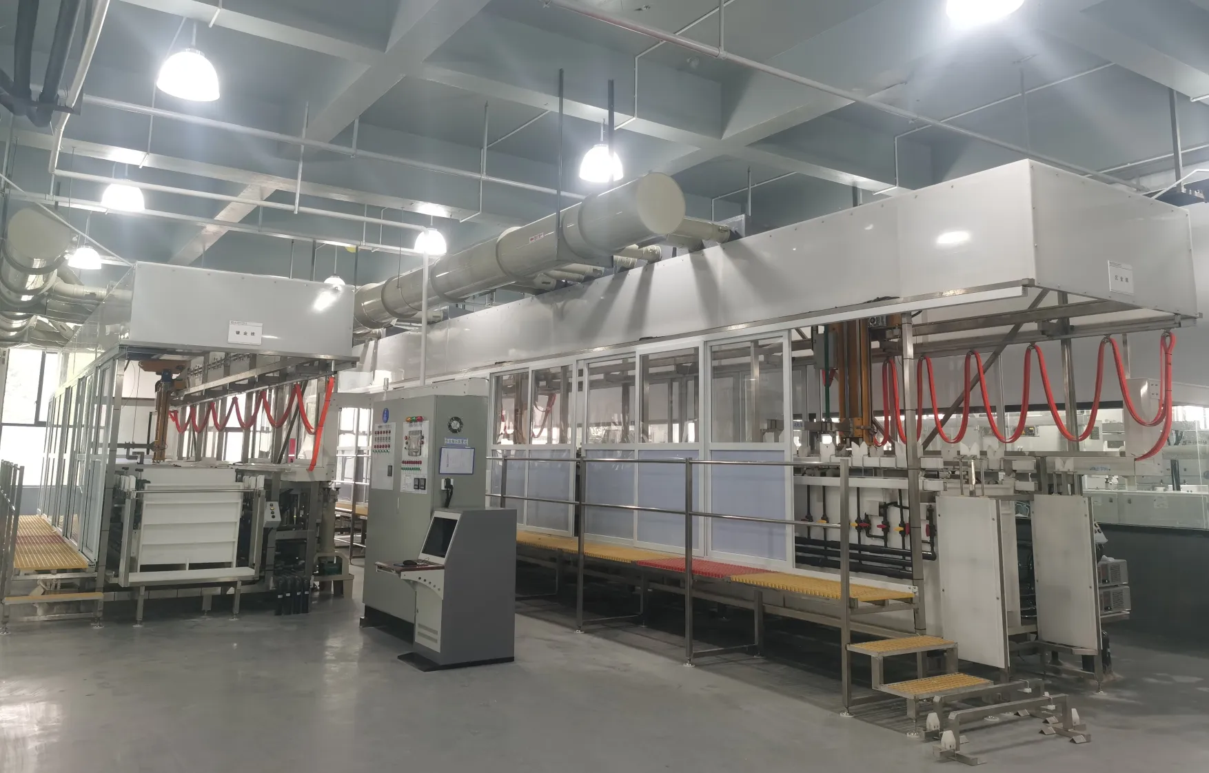
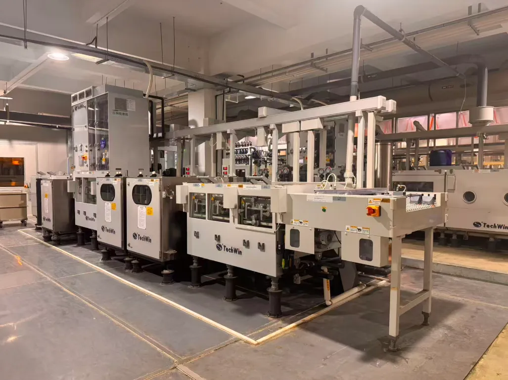
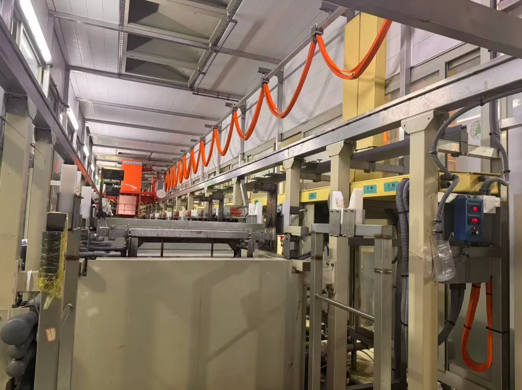
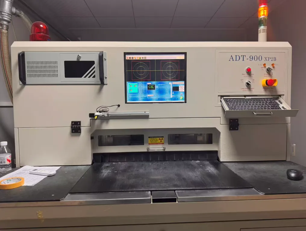
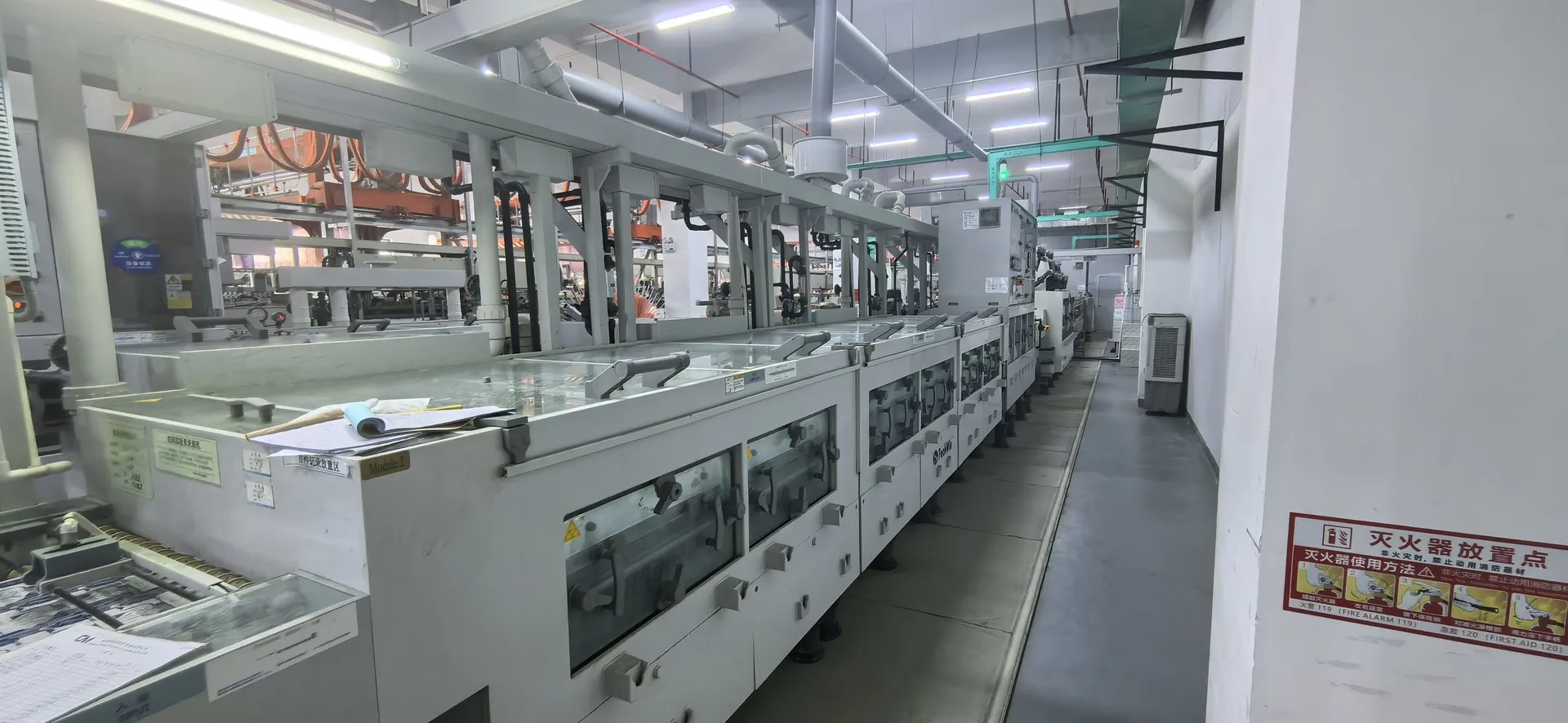
Production equipment
Selected equipment from the ShinePCB manufacturing network.
Factory-wide figures
| Item | Value |
|---|---|
| Max board size | 1 × 1 m |
| Pre-shipment inspection | 100% |
| In-house PCB laboratory | Supported, 20+ sets of equipment |
| PCB specialisation | High-frequency and high-speed PCB manufacturing |
| Quality inspection | AOI, X-ray, flying probe, impedance testing, final electrical test |
ShinePCB has established long-term cooperation with domestic and international laminate suppliers and PCB manufacturing facilities. Factory area, headcount and monthly capacity are not published until confirmed.